- 您现在的位置:买卖IC网 > Sheet目录1992 > DAC8531IDRBTG4 (Texas Instruments)IC D/A CONV LP 16-BIT 8-SON
DAC8531
12
SBAS192B
www.ti.com
OUTPUT AMPLIFIER
The output buffer amplifier is capable of generating rail-to-rail
voltages on its output which gives an output range of
0V to VDD. It is capable of driving a load of 2k in parallel with
1000pF to GND. The source and sink capabilities of the
output amplifier can be seen in the typical curves. The slew
rate is 1V/
s with a full-scale settling time of 8s with the
output unloaded.
The inverting input of the output amplifier is brought out to the
VFB pin. This allows for better accuracy in critical applications
by tying the VFB point and the amplifier output together
directly at the load. Other signal conditioning circuitry
may also be connected between these points for specific
applications.
SERIAL INTERFACE
The DAC8531 has a three-wire serial interface (SYNC,
SCLK, and DIN), which is compatible with SPI, QSPI, and
Microwire interface standards as well as most DSPs. See the
Serial Write Operation timing diagram for an example of a
typical write sequence.
The write sequence begins by bringing the SYNC line LOW.
Data from the DIN line is clocked into the 24-bit shift register
on the falling edge of SCLK. The serial clock frequency can
be as high as 30MHz, making the DAC8531 compatible with
high-speed (DSPs). On the 24th falling edge of the serial
clock, the last data bit is clocked in and the programmed
function is executed (i.e., a change in DAC register contents
and/or a change in the mode of operation).
At this point, the SYNC line may be kept LOW or brought
HIGH. In either case, it must be brought HIGH for a minimum
of 33ns before the next write sequence so that a falling edge
of SYNC can initiate the next write sequence. Since the
XXXX
X
PD1
PD0
D15
D14
D13
D12
D11
D10
D9
D8
D7
D6
D5
D4
D3
D2
D1
D0
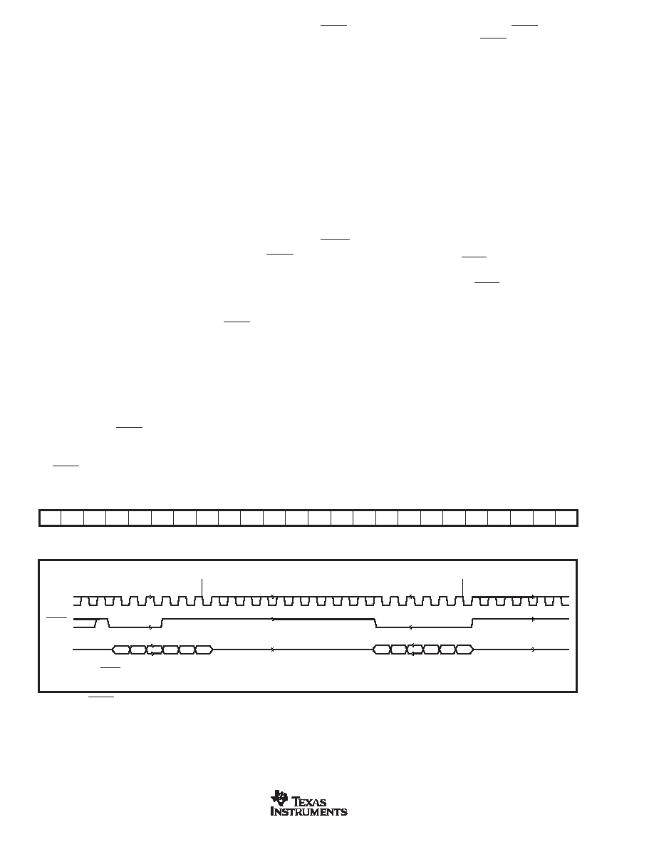
FIGURE 3. Data Input Register.
FIGURE 4. SYNC Interrupt Facility.
DB23
DB0
SYNC buffer draws more current when the SYNC signal is
HIGH than it does when it is LOW, SYNC should be idled
LOW between write sequences for lowest power operation of
the part. As mentioned above, it must be brought HIGH again
just before the next write sequence.
INPUT SHIFT REGISTER
The input shift register is 24 bits wide, as shown in Figure 3.
The first six bits are “don’t cares”. The next two bits (PD1 and
PD0) are control bits that control which mode of operation the
part is in (normal mode or any one of three power-down
modes). There is a more complete description of the various
modes in the Power-Down Modes section. The next 16 bits
are the data bits. These are transferred to the DAC register
on the 24th falling edge of SCLK.
SYNC INTERRUPT
In a normal write sequence, the SYNC line is kept LOW for
at least 24 falling edges of SCLK and the DAC is updated on
the 24th falling edge. However, if SYNC is brought HIGH
before the 24th falling edge, this acts as an interrupt to the
write sequence. The shift register is reset and the write
sequence is seen as invalid. Neither an update of the DAC
register contents or a change in the operating mode occurs,
as shown in Figure 4.
POWER-ON RESET
The DAC8531 contains a power-on reset circuit that controls
the output voltage during power-up. On power-up, the DAC
register is filled with zeros and the output voltage is 0V; it
remains there until a valid write sequence is made to the
DAC. This is useful in applications where it is important to
know the state of the output of the DAC while it is in the
process of powering up.
CLK
SYNC
D
IN
Invalid Write Sequence:
SYNC HIGH before 24th Falling Edge
Valid Write Sequence: Output Updates
on the 24th Falling Edge
DB23
DB0
DB23
DB0
24th Falling Edge
发布紧急采购,3分钟左右您将得到回复。
相关PDF资料
DAC8562FP
IC DAC 12BIT PARALLEL 5V 20-DIP
DS1004Z-5+T
IC DELAY LINE 5TAP 25NS 8-SOIC
DS1005-125+
IC DELAY LINE 5TAP 125NS 14-DIP
DS1007S-2+T&R
IC DELAY LINE 4NS 16-SOIC
DS1010S-50+T&R
IC DELAY LINE 10TAP 16-SOIC
DS1013S-25+T&R
IC DELAY LINE 25NS 16-SOIC
DS1020S-50+T
IC DELAY LINE 256TAP 16-SOIC
DS1021S-50+T&R
IC DELAY LINE 256TAP 16-SOIC
相关代理商/技术参数
DAC8532
制造商:BB 制造商全称:BB 功能描述:Dual Channel, Low Power, 16-Bit, Serial Input DIGITAL-TO-ANALOG CONVERTER
DAC8532IDGK
功能描述:数模转换器- DAC 16-Bit Dual Ch Low Power DAC RoHS:否 制造商:Texas Instruments 转换器数量:1 DAC 输出端数量:1 转换速率:2 MSPs 分辨率:16 bit 接口类型:QSPI, SPI, Serial (3-Wire, Microwire) 稳定时间:1 us 最大工作温度:+ 85 C 安装风格:SMD/SMT 封装 / 箱体:SOIC-14 封装:Tube
DAC8532IDGK
制造商:Texas Instruments 功能描述:16BIT DUAL DAC SMD 8532 MSOP8
DAC8532IDGKG4
功能描述:数模转换器- DAC 16-Bit Dual Ch Low Power DAC RoHS:否 制造商:Texas Instruments 转换器数量:1 DAC 输出端数量:1 转换速率:2 MSPs 分辨率:16 bit 接口类型:QSPI, SPI, Serial (3-Wire, Microwire) 稳定时间:1 us 最大工作温度:+ 85 C 安装风格:SMD/SMT 封装 / 箱体:SOIC-14 封装:Tube
DAC8532IDGKR
功能描述:数模转换器- DAC 16-Bit Dual Ch Low Power DAC RoHS:否 制造商:Texas Instruments 转换器数量:1 DAC 输出端数量:1 转换速率:2 MSPs 分辨率:16 bit 接口类型:QSPI, SPI, Serial (3-Wire, Microwire) 稳定时间:1 us 最大工作温度:+ 85 C 安装风格:SMD/SMT 封装 / 箱体:SOIC-14 封装:Tube
DAC8532IDGKRG4
功能描述:数模转换器- DAC 16-Bit Dual Ch Low Power DAC RoHS:否 制造商:Texas Instruments 转换器数量:1 DAC 输出端数量:1 转换速率:2 MSPs 分辨率:16 bit 接口类型:QSPI, SPI, Serial (3-Wire, Microwire) 稳定时间:1 us 最大工作温度:+ 85 C 安装风格:SMD/SMT 封装 / 箱体:SOIC-14 封装:Tube
DAC8534
制造商:TI 制造商全称:Texas Instruments 功能描述:Quad Channel, Low Power, 16-Bit, Serial Input DIGITAL-TO-ANALOG CONVERTER
DAC8534EVM
功能描述:数据转换 IC 开发工具 DAC8534 Eval Mod RoHS:否 制造商:Texas Instruments 产品:Demonstration Kits 类型:ADC 工具用于评估:ADS130E08 接口类型:SPI 工作电源电压:- 6 V to + 6 V